At TSMC’s North American Technology Symposium on Wednesday, the company detailed both its semiconductor technology and chip packaging technology roadmaps. While the former is key to keeping the traditional part of Moore’s Law going, the latter could accelerate a trend towards processors made from more and more silicon, leading quickly to systems the size of a full silicon wafer. Such a system, Tesla’s next generation Dojo training tile is already in production, TSMC says. And in 2027 the foundry plans to offer technology for more complex waferscale systems than Tesla’s that could deliver 40-times as much computing power as today’s systems.
For decades chipmakers increased the density of logic on processors largely by scaling down the area transistors take up and the size of interconnects. But that scheme has been running out of steam for a while now. Instead, the industry is turning to advanced packaging technology that allows a single processor to be made from a larger amount of silicon. The size of a single chip is hemmed in by the largest pattern lithography equipment can make. Called the reticle limit, that’s currently about 800 square millimeters. So if you want more silicon in your GPU you need to make it from two or more dies. The key is connecting those dies so that signals can go from one to the other as quickly and with as little energy as if they were all one big piece of silicon.
TSMC already makes a wafer-sized AI accelerator for Cerebras, but that arrangement appears to be unique and is different from what TSMC is now offering with what it calls System-on-Wafer.
In 2027, you can get a full wafer integration that delivers 40-times as much compute, more than 40 reticles worth of silicon and room for more than 60 high-bandwidth memory chips, TSMC predicts
For Cerebras, TSMC makes a wafer full of identical arrays of AI cores that are smaller than the reticle limit. It connects these arrays across the “scribe lines,” the areas between dies that are usually left blank, so the wafer can be diced up into chips. No chipmaking process is perfect, so there are always flawed parts on every wafer. But Cerebras designed in enough redundancy that it doesn’t matter to the finished computer.
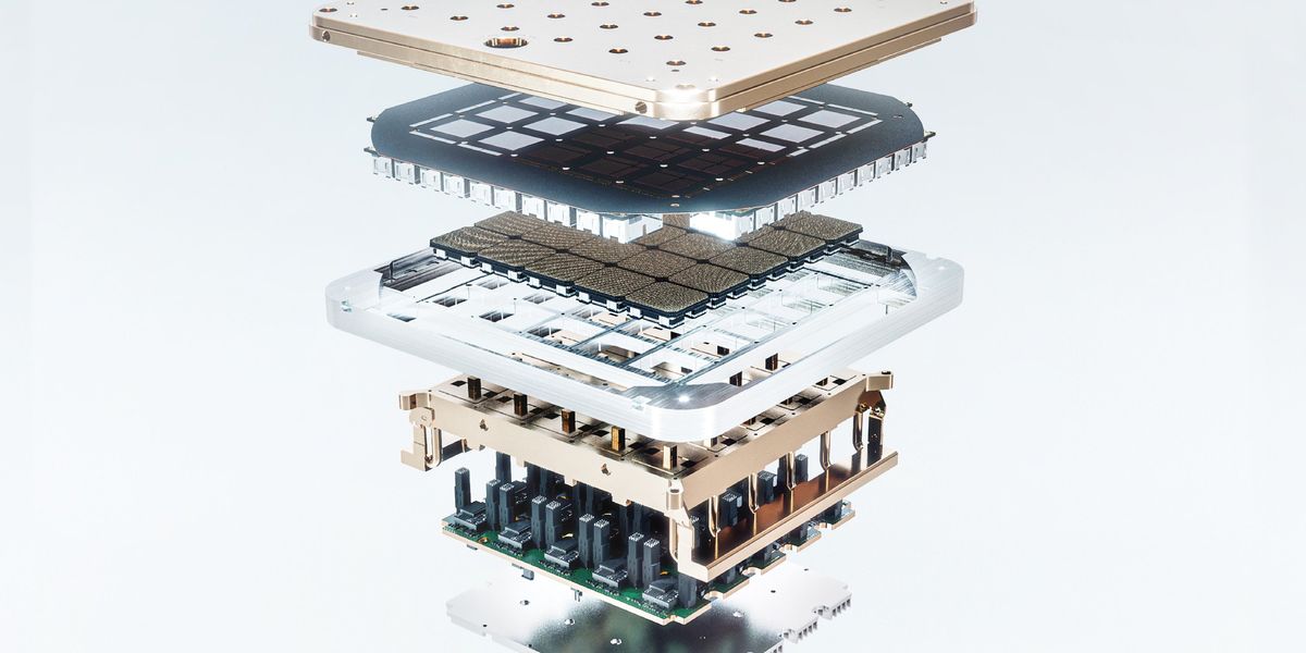
However, with its first round of System-on-Wafer, TSMC is offering a different solution to the problems of both reticle limit and yield. It starts with already tested logic dies to minimize defects. (Tesla’s Dojo contains a 5 x 5 grid of pretested processors.) These are placed on a carrier wafer, and the blank spots between the dies are filled in. Then a layer of high-density interconnects is constructed to connect the logic using TSMC’s integrated fan-out technology. The aim is to make data bandwidth among the dies so high that they effectively act like a single large chip.
By 2027, TSMC plans to offer waferscale integration based on its more advanced packaging technology, chip-on-wafer-on-substrate (CoWoS). In that technology, pre-tested logic and, importantly, high-bandwidth memory, is attached to a silicon substrate that’s been patterned with high-density interconnects and shot-through with vertical connections called through-silicon vias. The attached logic chips can also take advantage of the company’s 3D-chip technology called system-on-integrated chips (SoIC).
The waferscale version of CoWoS is the logical endpoint of an expansion of the packaging technology that’s already visible in top-end GPUs. Nvidia’s next GPU, Blackwell, uses CoWos to integrate more than 3-reticle-sizes worth of silicon, including 8 high-bandwidth memory (HBM) chips. By 2026, the company plans to expand that to 5.5-reticles, including 12 HBMs. TSMC says that would translate to more than 3.5 times as much compute power as its 2023 tech allows. But in 2027, you can get a full wafer integration that delivers 40-times as much compute, more than 40 reticles worth of silicon and room for more than 60 HBMs, TSMC predicts.
What waferscale is good for
The 2027 version of system-on-wafer somewhat resembles technology called Silicon-Interconnect Fabric, or Si-IF, developed at UCLA more than five years ago. The team behind SiIF includes electrical and computer engineering professor Puneet Gupta and IEEE Fellow Subramanian Iyer, who is now charged with implementing the packaging portion of the United States’ CHIPS Act.
Since then, they’ve been working to make the interconnects on the wafer more dense and to add other features to the technology. “If you want to this as a full technology infrastructure, it needs to do many other things beyond just providing fine pitch connectivity,” says Gupta, also an IEEE Fellow. “One of the biggest pain points for these large systems is going to be delivering power.” So the UCLA team is working on ways to add good quality capacitors and inductors to the silicon substrate and integrating gallium nitride power transistors.
AI training is the obvious first application for waferscale technology, but it is not the only one, and it may not even be the best, says University of Illinois Urbana-Champaign computer architect and IEEE Fellow Rakesh Kumar. At the International Symposium on Computer Architecture in June, his team is presenting a design for a waferscale network switch for data centers. Such a system could cut the number of advanced network switches in a very large—16,000-rack—data center from 4608 to just 48, the researchers report. A much smaller, enterprise-scale, data center for say 8,000 servers could get by using a single waferscale switch.